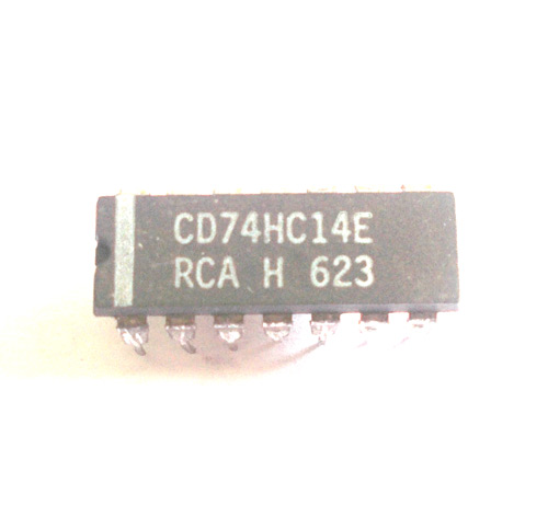
74HC14 – Hex Inverting Schmitt Trigger IC
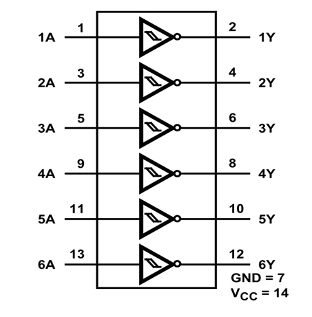
74HC14 is a member of 74XXXX series ICs, which consists of LOGIC GATES. 74HC14 IC has six NOT gates with SCHMITT TRIGGER. Hence name HEX INVERTING SCHMITT TRIGGER.
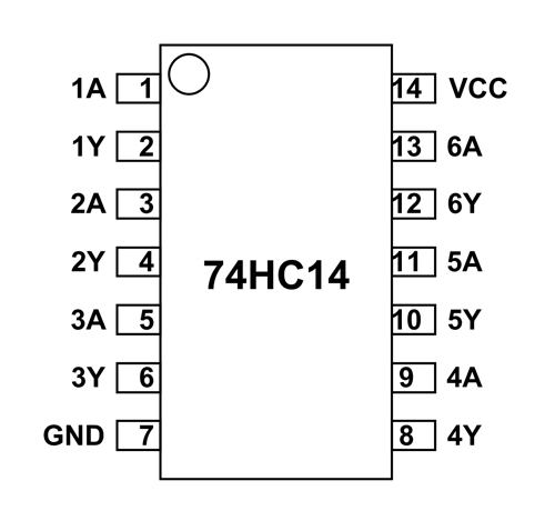
74HC14 Pin Configuration
As shown in the 74HC14 Pinout, it is a 14 PIN device which will be available in various packages choose the appropriate package depending on requirement. The description for each pin is given below.
|
Pin Number |
Description |
|
INPUT OF INVERTING SCHMITT TRIGGER GATE |
|
|
1 |
1A-INPUT of GATE 1 |
|
3 |
2A-INPUT of GATE 2 |
|
5 |
3A-INPUT of GATE 3 |
|
9 |
4A-INPUT of GATE 4 |
|
11 |
5A-INPUT of GATE 5 |
|
13 |
6A-INPUT of GATE 6 |
|
SHARED TERMINALS |
|
|
7 |
GND- Connected to ground |
|
14 |
VCC-Connected to positive voltage to provide power to all six gates |
|
OUTPUT OF INVERTING SCHMITT TRIGGER GATE |
|
|
2 |
1Y-OUTPUT of GATE 1 |
|
4 |
2Y-OUTPUT of GATE 2 |
|
6 |
3Y-OUTPUT of GATE 3 |
|
8 |
4Y-OUTPUT of GATE 4 |
|
10 |
5Y-OUTPUT of GATE 5 |
|
12 |
6Y-OUTPUT of GATE 6 |
74HC14 Features and Specifications
- Supply voltage range: -0.5V to +7.0V
- Maximum current allowed to draw through each gate output: 25mA
- Maximum total current allowed through VCC or GND pin: 50mA
- Totally lead free
- TTL outputs
- High noise immunity
- Maximum ESD: 2KV
- Typical Rise Time: 85-625ns (depending on supply voltage)
- Typical Fall Time: 85-625ns (depending on supply voltage)
- Operating temperature: -55°C to 125 °C
Note: Complete technical details can be found in the 74HC14 Datasheet linked at the bottom of this page.
74HC14 Equivalent ICs
MC14584, CD40106, Each op-amp can be configured to work as Schmitt trigger gate.
Where 74HC14 ICs Are Used?
For understanding the use of 74HC14 consider:
Case1: Where you want to convert signal waveforms to square wave. Schmitt trigger gates in 74HC14 can covert non-square wave forms to square waves. With Schmitt trigger gate we can convert sinusoidal or triangular wave to square wave.
Case2: When you want logic inverter. Inverter Schmitt triggers in this chip can provide output which is negated logic input. This chip gates can be used to get inverted logics for controllers or digital electronics.
Case3: When you want to eliminate noise in digital electronics. In digital electronics noise causes major errors in those cases using 74HC14 chip is ideal.
With multiple gates and fast output the 74HC14 usage is further promoted.
How to Use 74HC14
As mentioned earlier 74HC14 has six INVERTING SCHMITT TRIGGER GATES which can be used as six individual gates. The simplified internal structure can be given as below.
Now for understanding the usage of gate let us pick a single gate and connect the power to chip. Also Also provide an analog signal at the input.
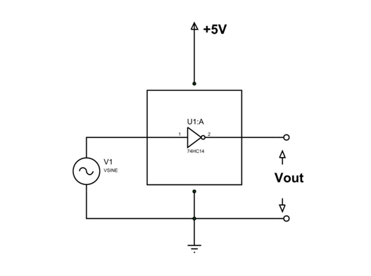
As shown in circuit, we are giving a sinusoidal wave at the input and taking Vout as output of gate. Once we draw the input and output graph we will have something like this.
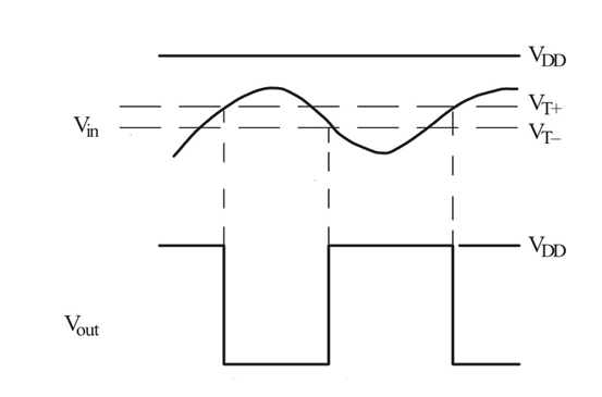
The Schmitt Trigger functioning principle is really simple, Inverting Schmitt Trigger output will be LOW only when input signal voltage level crosses its threshold voltage (+Vt).
As shown in figure, up to the point where Input voltage (Vin) reaches Threshold voltage (Vt+) the output voltage (Vout) is HIGH. Once it reaches threshold voltage, the output voltage goes LOW. Output voltage stays LOW until input voltage drops to low threshold voltage (Vt-). Once it reaches that point, the output voltage again goes HIGH. This cycle goes on.
As shown in graph, we can see when the sinusoidal signal is given as input we will have square wave output. We can use each gate like this to get the desired output.
Switching Time of 74HC14
The gates in 74HC14 take some time to provide output to the given input. These time delays are called switching times. Each gate will take time to turn ON and OFF. For understanding this better let us consider the switching diagram of a gate.
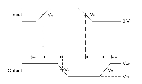
There are two delays which happen when switching. These two parameters are RISETIME (tPHL ) and FALLTIME (tPLH ).
In the graph, VoH goes LOW when INPUT reaches a threshold and VoH goes HIGH when INPUT goes lower than threshold voltage. In another sense it is the output voltage.
As you can see in the graph there is time delay between LOGIC INPUT going HIGH and VoH going LOW. This delay in providing response is called RISETIME (tPHL). The RISETIME (tPHL ) is 95ns.
Similarly in the graph there is time delay between LOGIC INPUT going LOW and VoH going HIGH at the OUTPUT. This delay in providing response is called FALLTIME (tPLH). The FALLTIME (tPLH) is 95ns.
Total is 192ns for each cycle. These delays must be considered at higher frequencies otherwise we will have major errors. Also there will be false triggering and noise beyond operating frequencies.
Applications
- General purpose logic
- PCs and notebooks
- TV, DVD, Set Top Box
- Networking
- Digital systems
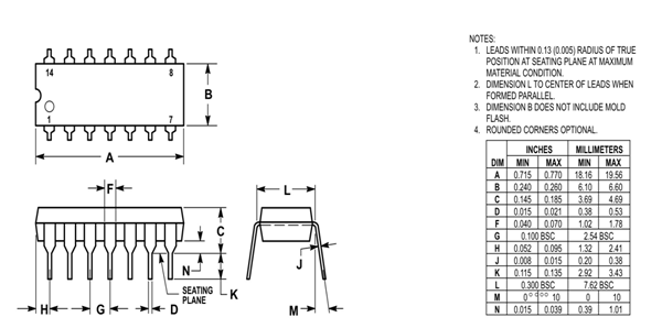
2D Model