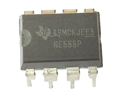
555 Timer IC
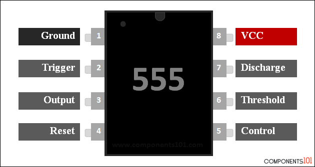
555 Timer Pinout Configuration
|
Pin Number |
Pin Name |
Description |
|
1 |
Ground |
Ground Reference Voltage 0V |
|
2 |
Trigger |
Responsible for transition of the flip-flop from set to reset. The output of the timer depends 2 I on the amplitude of the external trigger pulse applied to this pin |
|
3 |
Output |
This pin is normally connected to load as it is the only pin with output driven waveform |
|
4 |
Reset |
Negative pulse applied to this pin to disable or reset the timer. When not used for reset 4 I purposes, it should be connected to VCC to avoid false triggering |
|
5 |
Control |
Controls the threshold and trigger levels. It determines the pulse width of the output 5 Voltage I waveform. An external voltage applied to this pin can also be used to modulate the output waveform |
|
6 |
Threshold |
Compares the voltage applied to the terminal with a reference voltage of 2/3 Vcc. The 6 I amplitude of voltage applied to this terminal is responsible for the set state of the flip-flop |
|
7 |
Discharge |
Open collector output which discharges a capacitor between intervals (in phase with output). 7 I It toggles the output from high to low when voltage reaches 2/3 of the supply voltage |
|
8 |
Vcc |
Supply Voltage (Typical = 5V, Maximum = 18V) |
555 Timer IC Features
- Typical operating voltage is +5V, can withstand a maximum of +18V.
- The source/sink current of the output pin is 200mA
- Consumes up to 3mA when operating at +5V
- Trigger Voltage is 1.67 when operating at +5V
- Operating Temperature is 70 degree Celsius.
- Available in 8-pin PDIP, SOIC, and VSSOP packages
Note: The above values are mentioned for PDIP package, Complete Technical Details can be found in the 555 Timer datasheet given at the end of this page.
555 Timer IC Equivalent
LM556, NE556
Brief Description on 555 Timers
555 Timer IC is the most commonly used ICs for timing and Pulse generation applications. They can adopt itself into various applications due to its different operating modes. They are very simple to understand if we take a look at the components present inside as shown below
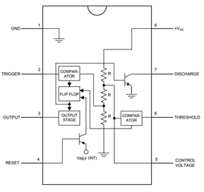
There are three resistors of value 5K, which gives this IC it’s iconic name “555 Timer”. It has dual comparators and flip-flop which will make this IC operated in three different modes such as Astable, Monostable and Bistable(Schimitt) Mode.
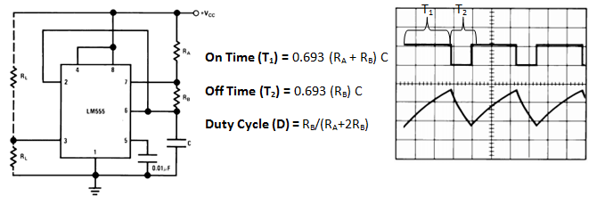
Astable Mode:
In this mode a square wave is produced at the output pin. This wave is usually used to turn ON and OFF a load at specific intervals like, blinking a LED. This mode is also used to generate clock pulse signals for digital IC’s. The ON time (T1) and OFF time (T2) of the wave can be controlled by the Resistors (RA, RB) and Capacitor (C) shown in below figure
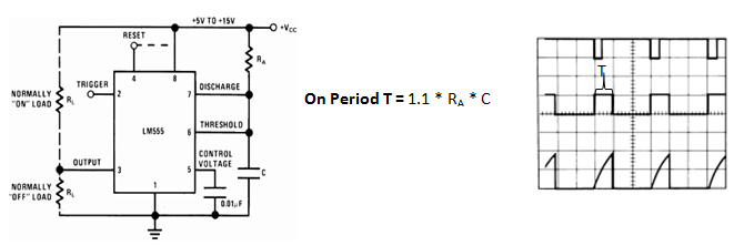
Monostable Mode:
In Monostable mode a pulse of pre-defined length is produced when a trigger button is pressed. The output pin stays low until the button is pressed and once pressed it remains high for a period of time decided by the value of resistor (RA) and Capacitor (C) shown in the below circuit.
Bi-Stable Mode:
The Bi-stable mode is also called as Schmitt Trigger Mode. This mode is used when a load has to be turned on and off using a push button. This mode does not have major practical importance hence it is rarely used.
Applications
- Time Delay Generation
- Pulse Width Modulation
- Pulse generation
- Precision Timing
- Sequential Timing circuits
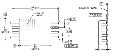
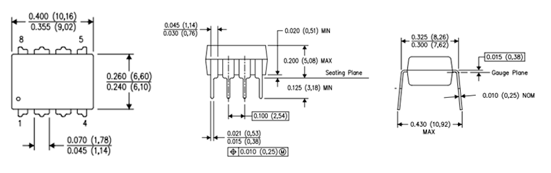
2D Model of 555 Timer IC
P-DIP Package
TSSOP Package: