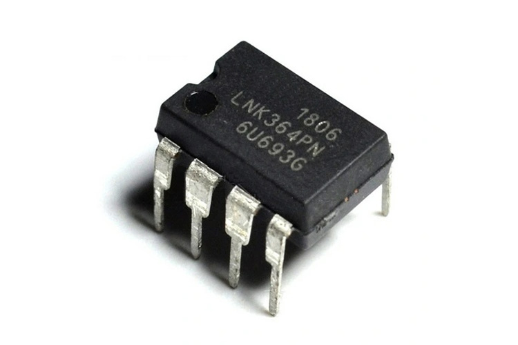
LNK364PN AC-DC Offline Switcher IC
The LNK364PN integrated circuit, a member of the LinkSwitch-TN family produced by Power Integrations, stands out for its utility in low-power, off-line switch mode power supplies. Characterized by an innovative design that combines a 700V power MOSFET with a controller on a single chip, it offers enhanced energy efficiency and reliability. This IC is distinguished by its ability to maintain a tight output regulation across a wide range of input voltages and load conditions, making it a versatile choice for applications such as chargers, adapters, and standby power supplies. The LNK364 incorporates numerous features aimed at minimizing external component count, thus simplifying the overall design and reducing costs. Notably, it includes auto-restart for short-circuit and open-loop protection, frequency jittering for lower EMI, and a high-voltage startup for improved system reliability. These attributes make the lnk 364 pn a robust and efficient solution for low-power applications, reflecting an integration of advanced circuit design and power management technology.
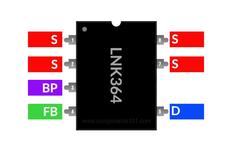
LNK364PN Pinout Configuration
| PIN | SYMBOL | DESCRIPTION | |
| LNK36xP/G | LNK36xD | ||
| 1,2,7,8 | 1,2,7,8 | S | Power MOSFET source connection |
| 3 | 1 | BP | Bypass pin, connect 0.1uF external bypass capacitor. |
| 4 | 2 | FB |
Feedback pin. |
| 5 | 4 | D | Power MOSFET drain connection. |
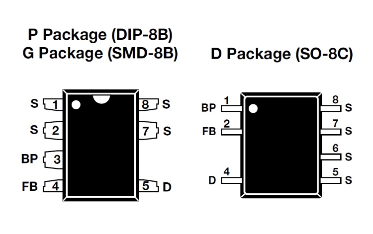
LNK364 Different Pinouts
Even though P ang G series LNK364 has the same pinout the D series has a different pinout. You can find the different pinouts below. It would help if you also kept this difference in mind while designing with LNK364.
LNK36x Variants
Within the LNK364x series, there are multiple parts available. Each variant has a different power handling capacity. Here are the available chip variants with their rated output power. The most popular among these variants are the lnk364gn and lnk364pn, more information about the same can be found in the lnk364 datasheet attached at the bottom of this page.
| OUTPUT POWER TABLE | ||||
| PRODUCT | 230 VAC ±15% | 85-265 VAC | ||
| ADAPTER | OPEN FRAME | ADAPTER | OPEN FRAME | |
| LNK362P/G/D | 2.8 W | 2.8 W | 2.6 W | 2.6 W |
| LNK363P/G/D | 5 W | 7.5 W | 3.7 W | 4.7 W |
| LNK364P/G/D | 5.5 W | 9 W | 54 W | 6 W |
Features of lnk364pn
- Proprietary IC trimming and transformer construction techniques enable Clampless designs with LNK364 for lower system cost, component count and higher efficiency.
- Fully integrated auto-restart for short circuit and open loop protection
- Self-biased supply – saves transformer auxiliary winding and associated bias supply components.
- Frequency jittering greatly reduces EMI.
- Meets HV creepage requirements between DRAIN and all other pins both on the PCB and at the package.
- Lowest component count switcher solution
- Accurate hysteretic thermal shutdown protection – automatic recovery improves field reliability.
- Universal input range allows worldwide operation.
- Simple ON/OFF control, no loop compensation needed.
- Eliminates bias winding – simpler, lower cost transformer.
- Very low component count – higher reliability and single side printed circuit board
- Auto-restart reduces delivered power by 95% during short circuit and open loop fault conditions.
- High bandwidth provides fast turn-on with no overshoot and excellent transient load response.
LNK364PN Equivalent ICs
LNK362, LNK363, LNK365, LNK366
Note: Complete technical details can be found in the LNK364 datasheet at this page’s end.
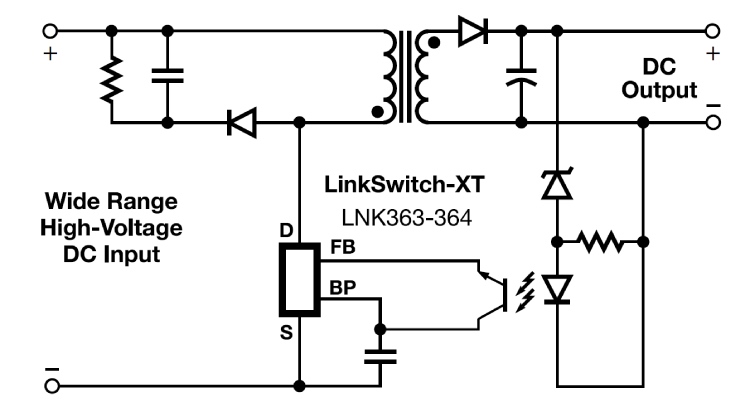
LNK364 Circuit Diargam
The image below shows the typical schematic diagram for a flyback converter with lnk 364 pn.
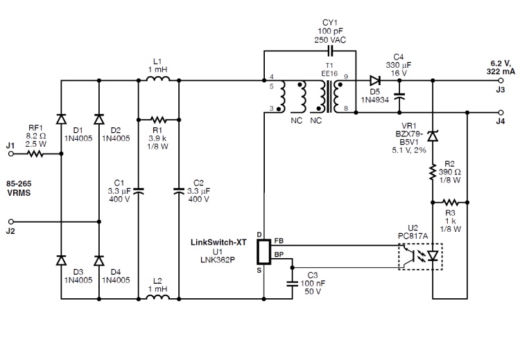
The circuit below is typical implementation of a universal input, 6.2 V, 322 mA adapter using ic lnk364pn. This circuit makes use of the clampless technique to eliminate the primary clamp components and reduce the cost and complexity of the circuit, making it cheaper to manufacture. The AC input side has the rectifier and filter circuit which is fed from the fusible inrush limit resistor. A pi filter is also added as differential mode noise attenuator. The low voltage output section contains the output rectifier and filter circuit along with the feed back circuit.
Applications
- Chargers/adapters for cell/cordless phones, PDAs, digital cameras, MP3/portable audio players, and shavers
- Supplies for appliances, industrial systems, and metering.
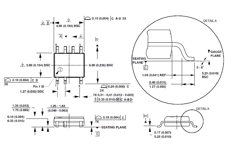
2D-Model and Dimensions
Below is the 2D CAD drawing of LNK364 along with its dimensions in inches (millimetres). The dimensions can be used to create custom footprints of the module and be used for PCB or CAD modelling.
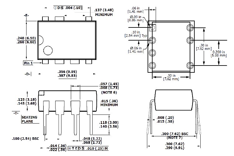
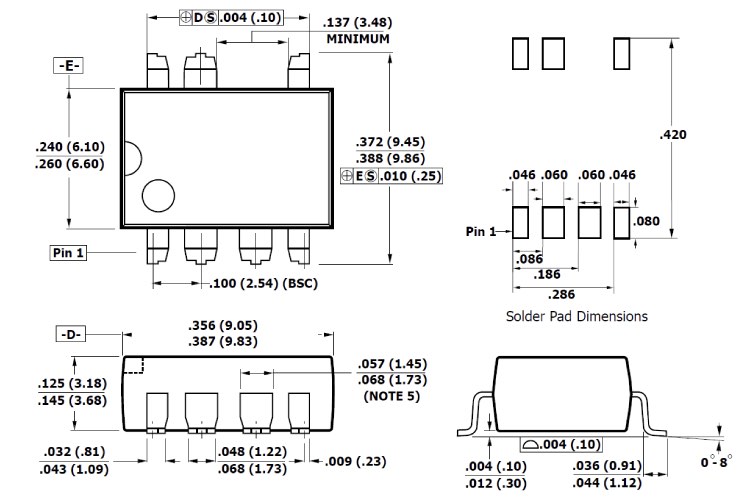
Dimensions are in millimeters (inches).