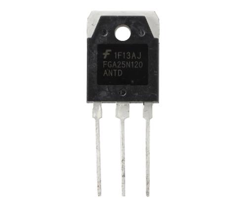
FGA25N120 IGBT
The FGA25N120 is a high voltage and high current IGBT with NPT Trench Technology. The IGBT can switch 1200V with a current rating of upto 50A. It also has a very low gate saturation voltage of 2V allowing it to be used in low voltage driver side designs.
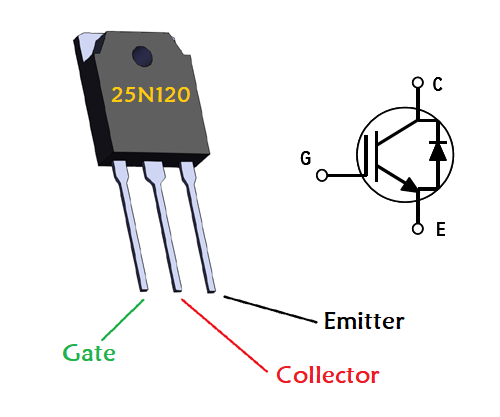
Pin Configuration
|
Pin Number |
Pin Name |
Description |
|
1 |
Gate |
Controls the biasing of the IGBT |
|
2 |
Collector |
Current flows in through Source |
|
3 |
Emitter |
Current flows out through Emitter |
Features
- High Voltage High Current IGBT with low saturation voltage
- Collector-Emitter Voltage (VCE): 1200V
- Collector Current (IC): 50A @25°C
- Minimum Gate threshold voltage (VGE) is 3.5V
- Maximum Gate threshold voltage (VGE) is 7.5V
- Gate-Emitter Voltage is (VGE) is ±20V (max)
- Rise time and fall time is about 60ns and 100ns respectively.
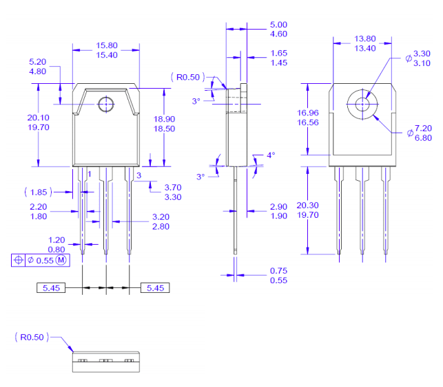
- Available in To-3P package
NOTE: Complete details can be found in the FGA25N120 IGBT Datasheet linked at the bottom of this page.
Alternatives for FGA25N120
FGA15N120, TA49123, FGA180N33
Where to use FGA25N120 IGBT?
The FGA25N120 is a high voltage high current IGBT, it can be used to switch high voltage values as high a 1200V with a current capability of 50A at 25°C. It can further handle high pulse currents of upto 90A making suitable in application where high voltage and switching current spikes are involved.
Since the IGBT uses Non Punch Though (NPT) Technology it has very low switching loss and low saturation voltage making it feasible to be used in low voltage switching driver designs and get comparatively high efficiency for its switching range. Like all IGBT’s the FGA25N also suffers from low switching speed and high voltage drop across collector and emitter compared with MOSFETs. So if you design requires high efficiency and faster switching device then you should prefer MOSFETs over IGBT. IGBT are preferred in designs where high switching voltage and current is involved.
How to use FGA25N120?
An IGBT is a combination of MOSFET and BJT, as we can notice from its pin-out. It has Gate on the input side similar to a MOSFET and Collector and Emitter on the output side similar to a BJT. This indicates that an IGBT is simply a MOSFET coupled with BJT on its output side to utilize the merits of a MOFET and BJT.
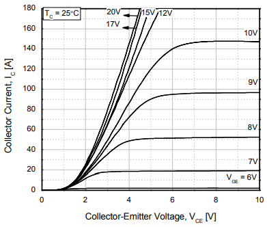
Similar to MOSFET, in IGBT also the gate pin has to be trigger with the minimum gate voltage to close the switch. Here in FGA25N120 the minimum gate saturation voltage is 2V but normally 5V is used in designs, the required gate trigger voltage can be calculated using the collector emitter voltage and collector current that has to be switched, using the graph in the datasheet as shown below
Once the gate is triggered the IGBT will remain on even after the trigger voltage is removed similar to a MOSFET. This is because of the gate capacitance present on the input gate pin of IGBT. To turn off the device the gate capacitance has to be discharged by simply connecting the gate pin of IGBT to ground. Because of this normally the Gate pin of IGBT is connected to ground though a pull down resistor of 10k or a gate driver IC like IR2104 is used.
When IGBT is used in switching circuits, care should be taken that it is not used in high frequency designs since the collector emitter voltage drop (switching loss) of the IGBT increase with increase in switching frequency. The graph for the same can be found in datasheet.
Applications
- High Voltage, high current switching devise
- Induction Heating
- Microwave Oven
- Large Solenoids
- Tesla Coils
- Converters or Inverter circuits
2D model of the component
If you are designing a PCB or Perf board with this component then the following picture from the 2N7000 Datasheet will be useful to know its package type and dimensions.