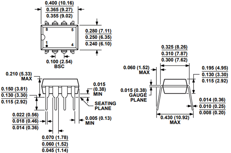
OP07 Single Operational Amplifier IC
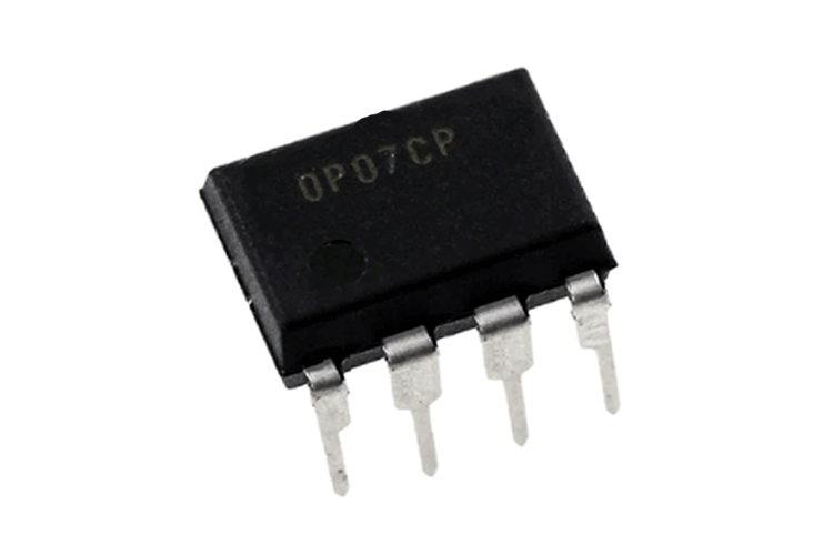

The OP07 is an Ultralow Offset Voltage ((75μV maximum) Operational Amplifier with low input bias current (±4nA) and high open-loop gain (200 V/mV). The OP07 is available in epoxy 8-lead PDIP and 8-lead narrow SOIC packages.
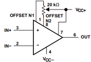
OP07 Pinout Configuration
|
Pin Number |
Pin Name |
Description |
|
1,8 |
VOS Trim |
Used to set offset voltage if required |
|
2 |
Inverting Input (IN-) |
The Inverting pin of the Op-Amp |
|
3 |
Non- Inverting Input (IN+) |
The Non-Inverting Pin of the Op-Amp |
|
4 |
V- |
Connected to negative rail or ground |
|
6 |
Output |
Output pin of the Op-Amp |
|
7 |
V+ |
Connected to the positive rail of supply voltage |
|
5 |
NC |
Not Connected |
OP07 features and specifications
- Low VOS: 75 µV (max.)
- Low VOS drift: 1.3 µV/°C (max.)
- Ultra-stable vs. time: 1.5 µV/month (max.)
- Low noise: 0.6 µV p-p (max.)
- Wide input voltage range: ±14 V
- Wide supply voltage range: ±3 V to ±18 V
- Fits 725, 108A/308A, 741, and AD510 sockets
- 125°C temperature-tested dice
- Available in 8-lead PDIP and 8-lead narrow SOIC packages
Note: Complete Technical Details can be found at the OP07 datasheet given at the end of this page.
Equivalent for OP07: UA741, CA3140, TL081, MC33171
Alternatives Audio Amplifiers: LM4871, AD620, IC6283, JRC45558, LF351
Where to use OP07 IC
The OP07 single operational amplifier offers a wide input voltage range of ±13 V minimum combined with a high CMRR of 106 dB and high input impedance to provide high accuracy in the noninverting circuit configuration. OP07 can maintain excellent linearity and gain accuracy even at high closed-loop gains. The OP07 has excellent Stability of offsets and gain with time or variations in temperature. These features made the OP07 an industry standard for instrumentation applications.
So if you are looking for an Op-Amp with wide input voltage range and higher stability and accuracy with temperature variations, then this IC might be the right choice for you.
How to Use OP07 IC
An Input Offset-Voltage Null Circuit from OP07 datasheet is given below. The input offset voltage of operational amplifiers caused by mismatched transistor pairs, collector currents, current gain betas (β), collector or emitter resistors, etc. These input mismatches can be adjusted by putting resistors or a potentiometer between the inputs as shown in the below circuit.
A 20K potentiometer is used between the offset null pins of the op-amp. This potentiometer is used to fine-tune the circuit during testing or for applications that require precision offset control.
Applications of OP07 Op Amp
- Wireless base station control circuits
- Optical network control circuits
- Instrumentation
- Sensors and controls
- Thermocouples
- Resistor thermal detectors (RTDs)
- Strain bridges
- Shunt current measurements
- Precision filters
2D-Model of OP07 (PDIP)