MCP16252 Boost Regulator
The MCP16252 is a compact, high-efficiency, fixed frequency, synchronous step-up DC-DC converter IC. This IC provides an easy-to-use power supply solution for applications powered by either one-cell, two-cell or three-cell alkaline, NiCd, NiMH, one-cell Li-Ion or Li-Polymer batteries.
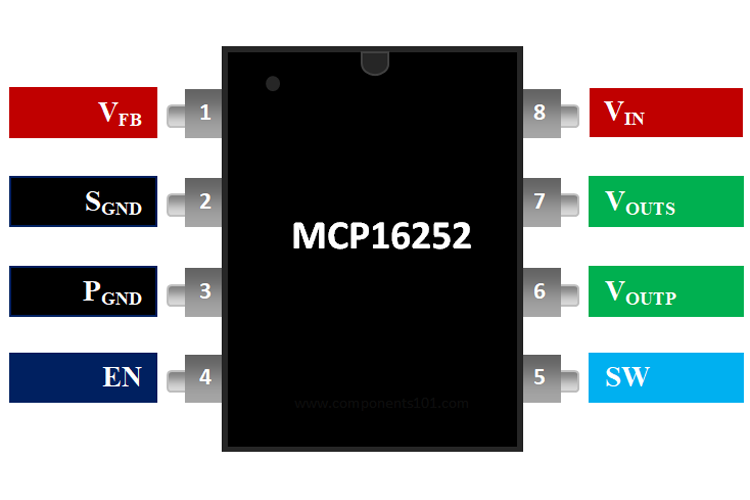
Pin Configuration of MCP16252
|
Pin Number |
Pin Name |
Description |
|
1 |
VFB |
Feedback Voltage Pin |
|
2 |
SGND |
Signal Ground Pin |
|
3 |
PGND |
Power Ground Pin |
|
4 |
EN |
Enable Control Input Pin |
|
5 |
SW |
Switch Node, Boost Inductor Input Pin |
|
6 |
VOUTP |
Output Voltage Power Pin |
|
7 |
VOUTS |
Output Voltage Sense Pin |
|
8 |
VIN |
Input Voltage Pin |
Features & Specifications of MCP16252
- Number of Outputs: 1 Output
- Input Voltage Range: 0.82V to 5.5V
- Output Voltage: 1.8V to 5.5V
- Current – Output: 100mA
- Frequency – Switching: 500kHz
- Load Regulation: 1.5 %
- Shutdown Current: 0.6 µA typical
- Feedback Voltage: 1.23V
- Available in SOT-23, 6-Lead- TDFN, 2 x 3 x 0.8 mm, 8-Lead
Note: Complete Technical Details can be found at the MCP16252 datasheet given at the end of this page.
MCP16252 Equivalent
ACT4514, CS51411, TS2580
Alternative DC-DC Controllers
Where to use MCP16252
The MCP16252 is a synchronous step-up DC-DC converter IC, which is normally used in One, Two and Three-Cell Alkaline and NiMH/NiCd Portable Products. Since the regulation occurs through switching it is very efficient than linear circuits. The internal oscillator supports the switching frequencies from 425 kHz to 575 kHz.
The input voltage for the IC is from 0.82V to 5.5V and the output voltage can be varied from 1.8V to 5.5V and the maximum output current can be up to 100mA. So if you looking to design a DC-DC converter with the above specifications then MCP16252 might be of interest to you.
How to use MCP16252
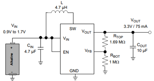
This IC requires a minimum number of components to be operational. A test circuit diagram from the MCP16252 datasheet is given below. As shown in the circuit diagram output voltage is set by a small external resistor divider. VIN pin is connected to the input voltage source. The input source should be decoupled to GND with a 4.7 µF minimum capacitor. The VFB pin is used to provide output voltage regulation by using a resistor divider
Applications of MCP16252
- One, Two and Three-Cell Alkaline and NiMH/NiCd
- Portable Products
- Solar Cell Applications
- Personal Care and Medical Products
- Bias for Status LEDs
- Smartphones, MP3 Players, Digital Cameras
- Remote Controllers, Portable Instruments
- Wireless Sensors
- Bluetooth Headsets
- +3.3V to +5.0V Distributed Power Supply
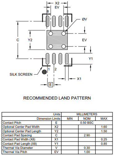
2D Model of MCP16252
Dimensions for MCP16252IC are given below. These dimensions are for the SOIC package. If you are using different package IC please refer to the MCP16252 datasheet.