CD4068B 8-Input NAND/AND Gate
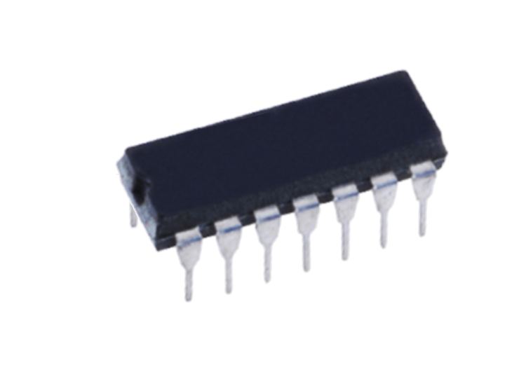
The CD4068B is a NAND/AND gate IC with direct implementation of the positive logic 8-input NAND and AND functions and supplements the existing family of CMOS gates. The CD4068B is available in DIP and SOP packages.
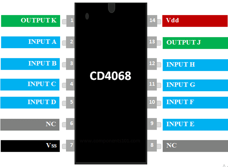
Pin Description of CD4068B
|
Pin No. |
Pin Name |
Function |
|
2, 3, 4, 5, 9,10, 11, 12 |
A, B, C, D, E, F, G, H |
Data Inputs |
|
6, 8 |
NC |
Not Connected |
|
1 |
K |
Data Output (AND) |
|
13 |
J |
Data Output (NAND |
|
7 |
Vss |
Negative Supply Voltage |
|
14 |
Vdd |
Positive Supply Voltage |
Features of CD4068B:
- 8-input NAND/AND Gate
- Operating Voltage: 3V to 18V
- Output current High: -1.5mA
- Output current Low: 1.5mA
- Operating Temperature: -55 to 125°C
- Propagation Delay: 75 nS
- Available in 14-pin PDIP, GDIP, PDSO packages
Note: Complete Technical Details can be found at the CD4068B datasheet give at the end of this page.
Equivalent for CD4068: HCF4068
NAND/AND Gate Truth Table:
Truth tables for both 8-input AND/NAND gate are given below. Boolean Function functions of NAND and AND gate are the opposite.
|
INPUTS |
OUTPUT
|
|||||||
|
A |
B |
C |
D |
E |
F |
G |
H |
J (NAND) |
|
L |
X |
X |
X |
X |
X |
X |
X |
H |
|
X |
L |
X |
X |
X |
X |
X |
X |
H |
|
X |
X |
L |
X |
X |
X |
X |
X |
H |
|
X |
X |
X |
L |
X |
X |
X |
X |
H |
|
X |
X |
X |
X |
L |
X |
X |
X |
H |
|
X |
X |
X |
X |
X |
L |
X |
X |
H |
|
X |
X |
X |
X |
X |
X |
L |
X |
H |
|
X |
X |
X |
X |
X |
X |
X |
L |
H |
|
H |
H |
H |
H |
H |
H |
H |
H |
L |
|
INPUTS |
OUTPUT
|
|||||||
|
A |
B |
C |
D |
E |
F |
G |
H |
J (AND) |
|
L |
X |
X |
X |
X |
X |
X |
X |
L |
|
X |
L |
X |
X |
X |
X |
X |
X |
L |
|
X |
X |
L |
X |
X |
X |
X |
X |
L |
|
X |
X |
X |
L |
X |
X |
X |
X |
L |
|
X |
X |
X |
X |
L |
X |
X |
X |
L |
|
X |
X |
X |
X |
X |
L |
X |
X |
L |
|
X |
X |
X |
X |
X |
X |
L |
X |
L |
|
X |
X |
X |
X |
X |
X |
X |
L |
L |
|
H |
H |
H |
H |
H |
H |
H |
H |
H |
How to use CD4068:
TO use the CD4068 IC, just power it using the Vcc (pin 14) and ground (pin 7) lines. The typical operating voltage of the IC is +5V, but it can also be operated in +5V, +10V, and +15V. The output voltage of the IC on the pin J and K will be equal to the operating voltage of the IC. As per the truth table is shown above, the NAND gate will be high in every condition except the last one in which all the inputs are high. On the other hand AND gate will be LOW in every condition except the last condition when all the inputs are high.
Applications of CD4068B:
- Logic Buffer circuit
- Basic Logic Circuits
- Encoders and Decoders
- Multiplexers and De-multiplexers
- Oscillator circuits
- Networking and Digital Systems
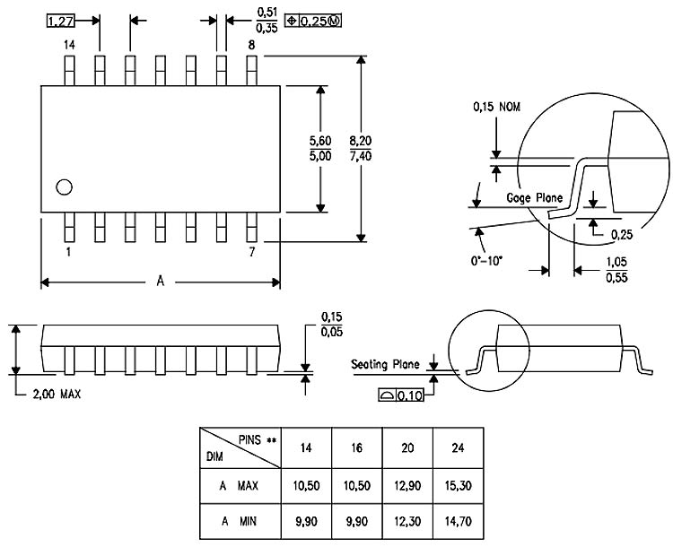
2D-Model of CD4068B:
Dimensions for CD4068B IC is given below. These dimensions are for the PDSO package. If you are using different package IC please refer to the CD4068B datasheet.