Capable of supporting up to 32 GT/s without altering design
Fundamentals of MOSFETs and Their Working
Power Electronic Switching components like BJT, MOSFET, IGBT, SCR, TRIAC, etc. are essential devices used in the design of many circuits ranging from a simple driver circuit to complex Power rectifiers and Inverters. The most basic of them all is the BJT, and we have already learned the working of BJT Transistors. Next to BJT, the widely used power switches are MOSFETs. Compared to BJT, MOSFET can handle high voltage and high current, hence it is popular among high power applications. In this article, we will learn the Basics of MOSFET, its internal construction, how it works, and how to use them in your circuit designs. If you want to skip the theory, you can check out the article on popular MOSFETs and where to use them to speed your part selection and design process.
What is a MOSFET?
MOSFET stands for Metal Oxide Field Effect Transistor, MOSFET was invented to overcome the disadvantages present in FETs like high drain resistance, moderate input impedance, and slower operation. So a MOSFET can be called the advanced form of FET. In some cases, MOSFETs are also be called IGFET (Insulated Gate Field Effect Transistor). Practically speaking, MOSFET is a voltage-controlled device, meaning by applying a rated voltage to the gate pin, the MOSFET will start conducting through the Drain and Source pin. We will get into details later in this article.
The main difference between FET and MOSFET is that MOSFET has a Metal Oxide Gate electrode electrically insulated from the main semiconductor n-channel or p-channel by a thin layer of Silicon dioxide or glass. The isolation of the controlling Gate increases the input resistance of the MOSFET extremely high in the value of the Mega-ohms (MΩ).
Symbol Of MOSFET
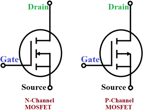
In general, the MOSFET is a four-terminal device with a Drain (D), Source (S), gate (G) and a Body (B) / Substrate terminals. The body terminal will always be connected to the source terminal hence, the MOSFET will operate as a three-terminal device. In the below image, the symbol of N-Channel MOSFET is shown on the left and the symbol of P-Channel MOSFET is shown on the right.
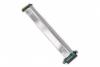
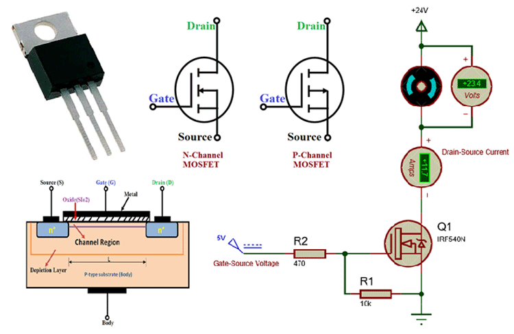
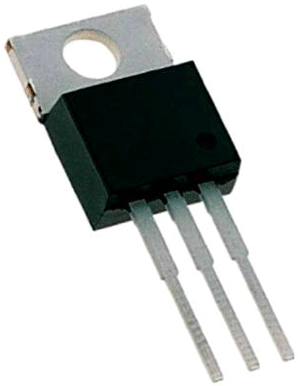
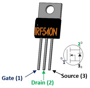
The most commonly used package for MOSFET is To-220, for a better understanding let’s take a look at the pinout of the famous IRF540N MOSFET (shown below). As you can see the Gate, Drain, and Source pin are listed below, do remember that the order of these pins will change based on the manufacturer. The other popular MOSFETs are IRFZ44N, BS170, IRF520, 2N7000, etc
MOSFET as a Switch
The most common application of a MOSFET is using it as a switch. The below circuit shows the MOSFET operating as a Switching device for turning ON and OFF of the lamp. The gate input voltage VGS applied with the help of an input voltage source. When the applied voltage is positive, the motor will be in the ON state and if the applied voltage is zero or negative, the lamp will be in OFF state.
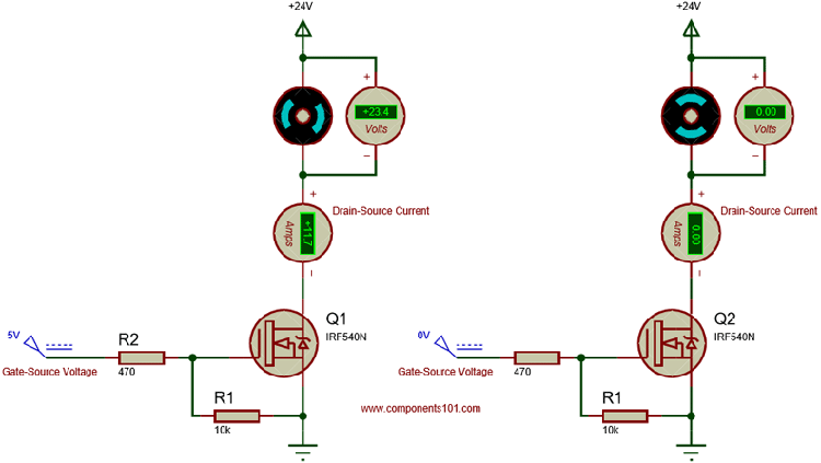
When you turn on a Mosfet by supplying the required voltage to the gate pin, it will remain on unless you supply 0V to the gate. To avoid this problem, we should always use a pull-down resistor (R1), here I have used a value of 10k. In applications like controlling the speed of the motor or dimming light, we would use a PWM signal for fast switching, during this scenario the MOSFET’s gate capacitance will create a reverse current due to parasitic effect. To tackle this, we should use a current limiting capacitor, I have used a value of 470 here.
The above load is considered as a resistive load, hence the circuit is very simple, and in case we need to use an inductive or capacitive load, we need to use some kind of protection to prevent the MOSFET from getting damaged. For example, if we use a capacitive load without an electric charge it is considered as a short circuit, this will result in a high “inrush” of current and when the applied voltage is removed from an inductive load, there will be a large amount of reverse voltage buildup in the circuit when the magnetic field collapses, it will lead to an induced back-emf in the winding of the inductor.
Classification of MOSFET
The MOSFET is Classified into two types based on the type of operations, namely Enhancement mode MOSFET (E-MOSFET) and Depletion mode MOSFET (D-MOSFET), these MOSFETs are further classified based on the material used for construction as n-channel and p-channel. So, in general, there are 4 different types of MOSFETs
- N-Channel Depletion mode MOSFET
- P-Channel Depletion mode MOSFET
- N-Channel Enhancement mode MOSFET
- P-Channel Enhancement mode MOSFET
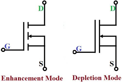
The N-channel MOSFETs are called NMOS and they are represented by the following symbols.
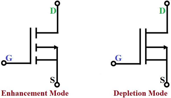
According to the internal construction of a MOSFET, the Gate(G), Drain (D), and Source(S) pins are physically connected in a Depletion Mode MOSFET, while they are physically separated in Enhancement Mode, this is the reason why the symbol appears broken for an Enhancement Mode MOSFET. The P-Channel MOSFETs are called PMOS and they are represented by the following symbols.
Of the available types, the N-Channel Enhancement MOSFET is the most commonly used MOSFET. But for the sake of knowledge let's try to get into the difference. The main difference between the N-Channel MOSFET and P-Channel MOSFET is that in an N-channel, the MOSFET switch will remain open until a gate voltage is provided. When the gate pin receives the voltage, the switch (between Drain and Source) will get closed and in P-Channel MOSFET the switch will remain closed until a gate voltage provided.
Similarly, the main difference between the Enhancement Mode and Depletion Mode MOSFET is that Gate voltage applied to E-MOSFET should always be positive and it has a threshold voltage above which it turns on completely. For a D-MOSFET the gate voltage can either be positive or negative and it never turns on completely. Also note that a D-MOSFET can work in Enhancement and Depletion mode, while an E-MOSFET can work only in Enhancement mode.
Construction Of MOSFET
The below image shows the typical internal structure of the MOSFET. Although the MOSFET is an advanced form of FET and operates with the same three terminals as a FET the internal structure of the MOSFET is really different from the general FET.
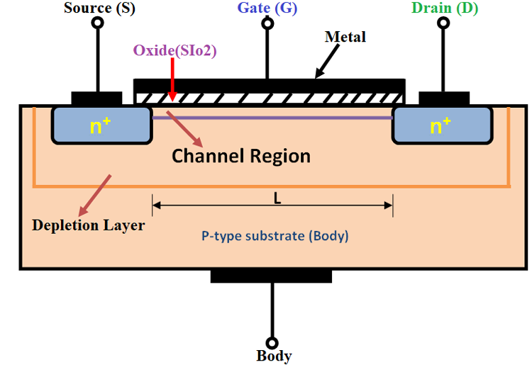
If you look at the structure, you could see that the gate terminal is fixed on the thin metal layer which is insulated by a layer of Silicon Dioxide (SiO2) from the semiconductor, and you will be able to see two N-type semiconductors fixed in the channel region where the drain and source terminals are placed. The channel between the drain and source of the MOSFET is an N-type, opposite to this, the substrate is implemented as P-type. This helps in biasing MOSFET in both the polarities, either positive or negative. If the gate terminal of the MOSFET isn’t biased, it will stay in the non-conductive state, hence the MOSFET is mostly used in designing switches and logic gates.
Working Principle of MOSFET
In general, the MOSFET works as a switch, the MOSFET controls the voltage and current flow between the source and drain. The working of the MOSFET depends on the MOS capacitor, which is the semiconductor surface below the oxide layers between the source and drain terminal. It can be inverted from p-type to n-type, simply by applying positive or negative gate voltage respectively. The below image shows the block diagram of the MOSFET.
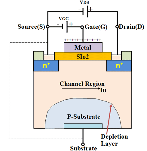
When a drain-source voltage (VDS) is connected between the drain and source, a positive voltage is applied to the Drain, and the negative voltage is applied to the Source. Here the PN junction at the drain is reverse biased and the PN junction at the Source is forward biased. At this stage, there will not be any current flow between the drain and the source.
If we apply a positive voltage (VGG) to the gate terminal, due to electrostatic attraction the minority charge carriers (electrons) in the P substrate will start to accumulate on the gate contact which forms a conductive bridge between the two n+ regions. The number of free electrons accumulated at the gate contact depends on the strength of positive voltage applied. The higher the applied voltage greater the width of the n-channel formed due to electron accumulation, this eventually increases the conductivity and the drain current (ID) will start to flow between the Source and Drain.
When there is no voltage applied to the gate terminal, there will not be any current flow apart from a small amount of current due to minority charge carriers. The minimum voltage at which the MOSFET starts conducting is called the threshold voltage.
Operation of MOSFET in Depletion Mode:
The depletion-mode MOSFETs are usually called the “Switched ON” devices as they are generally in the closed state when there is no bias voltage at the gate terminal. When we increase the applied voltage to the gate in positive the channel width will be increased in depletion mode. This will increase the drain current ID through the channel. If the applied gate voltage is highly negative, then the channel width will be less and the MOSFET might enter into the cutoff region.
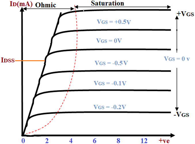
VI characteristics:
The V-I characteristics of the depletion-mode MOSFET transistor are drawn between the drain-source voltage (VDS) and Drain current (ID). The small amount of voltage at the gate terminal will control the current flow through the channel. The channel formed between the drain and the source will act as a good conductor with zero bias voltage at the gate terminal. The channel width and drain current will increase if the positive voltage is applied to the gate whereas they will get decreased when we apply a negative voltage to the gate.
Operation of MOSFET in Enhancement Mode:
The operation of MOSFET in Enhancement mode is similar to the operation of the open switch, it will start to conduct only if the positive voltage(+VGS) is applied to the gate terminal and the drain current starts to flow through the device. The channel width and drain current will increase when the bias voltage increases. But if the applied bias voltage is zero or negative the transistor will remain in the OFF state itself.
VI Characteristics:
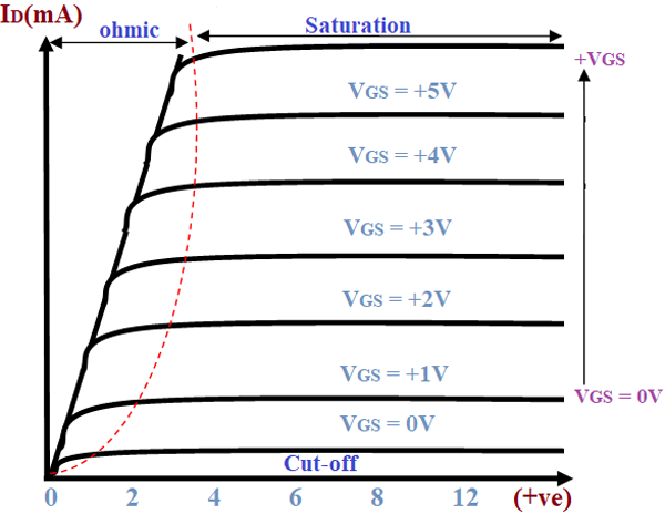
VI characteristics of the enhancement-mode MOSFET are drawn between the drain current (ID) and the drain-source voltage (VDS). The VI characteristics are partitioned into three different regions, namely ohmic, saturation, and cut-off regions. The cutoff region is the region where the MOSFET will be in the OFF state where the applied bias voltage is zero. When the bias voltage is applied, the MOSFET slowly moves towards conduction mode, and the slow increase in conductivity takes place in the ohmic region. Finally, the saturation region is where the positive voltage is applied constantly and the MOSFET will be staying in the conduction state.
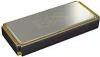
Packages of MOSFET
MOSFETs are available in different packages, sizes, and names for their usage in different kinds of applications. In general, MOSFETs delivered in 4 different packages, namely, surface mount, Thru-Hole, PQFN, and DirectFET
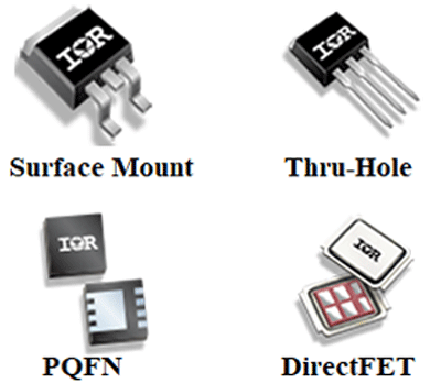
The MOSFETs are available with a different name in each kind of packages as follows:
Surface Mount: TO-263, TO-252, MO-187, SO-8, SOT-223, SOT-23, TSOP-6, etc.
Thru-Hole: TO-262, TO-251, TO-274, TO-220, TO-247, etc.
PQFN: PQFN 2x2, PQFN 3x3, PQFN 3.3x3.3, PQFN 5x4, PQFN 5x6, etc.
DirectFET : DirectFET M4, DirectFET MA, DirectFET MD, DirectFET ME, DirectFET S1, DirectFET SH, etc.